 2020, Vol. 38
Institute of Oceanology, Chinese Academy of Sciences
Article Information
- TIAN Jing, CHEN Zhuoyuan, JING Jiangping, FENG Chang, SUN Mengmeng, LI Weibing
- Photoelectrochemical cathodic protection of Cu2O/TiO2 p-n heterojunction under visible light
- Journal of Oceanology and Limnology, 38(5): 1517-1531
- http://dx.doi.org/10.1007/s00343-020-9327-y
Article History
- Received Dec. 19, 2019
- accepted in principle Jan. 30, 2020
- accepted for publication Mar. 16, 2020


2 School of Environment and Safety Engineering, Qingdao University of Science and Technology, Qingdao 266042, China;
3 Center for Ocean Mega-Science, Chinese Academy of Sciences, Qingdao 266071, China;
4 University of Chinese Academy of Sciences, Beijing 100049, China
Metallic corrosion can cause huge economic losses and great harm to human's living environments. Traditional anti-corrosion technologies, such as organic coating and cathodic protection, cause not only waste of resources and energy, but also environmental pollution. The photoelectrochemical cathodic protection (PECCP) technology couples semiconductor materials with metallic materials and transfers the photoinduced electrons generated by the semiconductor materials under light illumination to the metallic materials to protect them. Therefore, the PECCP technology is considered an environmentally friendly novel corrosion protection technology (Bu et al., 2018). Semiconductor materials that can be used for PECCP mainly include TiO2 (Ohko et al., 2001; Sun et al., 2013; Momeni et al., 2019a), ZnO (Sun et al., 2014; Yang and Cheng, 2018), SrTiO3 (Yang and Cheng, 2017), and g-C3N4 (Bu et al., 2013; Jing et al., 2019b). Among them, TiO2 has been widely used in photocatalytic degradation of organic pollutants (Zhuang et al., 2010), dye-sensitized solar cells (Roy et al., 2010; Sauvage et al., 2010), supercapacitors (Lu et al., 2012, 2013), photocatalytic sterilization (Foster et al., 2011; Yadav et al., 2014), photocatalytic hydrogen production (Kho et al., 2010; Xiang et al., 2012), and in other fields since the photoelectric conversion effect was found by Fujishima and Honda (1972). In addition, TiO2 is of low cost, easy preparation, and good stability, and can control the directional migration of photogenerated electrons through the regulation of one-dimensional (1D) nanorods and nanotubes. However, as a wide-bandgap semiconductor, TiO2 can only response to ultraviolet light, which limits its applications in the areas of photocatalysis (Momeni, 2015; Momeni et al., 2015), PECCP and dye-sensitized solar cell. Therefore, the main methods to broaden the application of TiO2 are to extend the light absorption of TiO2 to visible region and to make it use solar energy effectively.
At present, the main methods for expanding the light absorption range of a semiconductor material are metallic elements doping (Kočí et al., 2010; Tian et al., 2012; Momeni et al., 2018; Momeni et al., 2019b), non-metallic elements doping (Zhang et al., 2011; Momeni et al., 2019c), introduction of defects (Dong et al., 2014; Tian et al., 2018), and compounding with other semiconductors possessing narrow bandgap (Yan and Yang, 2011; Zhang et al., 2012; Chen et al., 2014a; Sun et al., 2018). The metallic and non-metallic elements doping will introduce doping levels in the bandgap of a semiconductor, thereby narrowing the forbidden bandwidth of the semiconductor and broadening the response range of light. The introduction of defects will also reduce the forbidden bandwidth of the semiconductor through introducing the defect levels, thereby broadening the light response range of the semiconductor. The compounding with other semiconductors having narrow bandgap increases the light response capability. Meanwhile, the heterojunction system will form at the interface of different semiconductors, which can increase the separation efficiency of the photogenerated carriers. Therefore, more photogenerated carriers can be separated and participate in the chemical reactions. Zhang et al. (2012) prepared Bi2S3/Bi2WO6 composite photocatalyst by one-step hydrothermal method. The coupling of narrow-bandgap Bi2S3 extended the light absorption threshold of Bi2WO6 from 450 nm to 800 nm, and the heterojunction formed at the interface of Bi2S3/Bi2WO6 efficiently separated the photogenerated electrons and holes, which made the phenol degradation rate of Bi2S3/Bi2WO6 be 6.2 times higher than that of pure Bi2WO6. Gou et al. (2017) prepared zeolite-supported Ag2O/TiO2 composites with excellent photocatalytic degradation performance of norfloxacin by improved sol-gel method. The high photocatalytic performance is attributed to the enhanced visible light absorption and high charge separation efficiency because of the combination of the narrow-band gap semiconductor.
In addition to the abovementioned Bi2S3 and Ag2O, Cu2O, as a narrow-bandgap semiconductor (2– 2.2 eV), has good visible light absorption performance and is widely used in the field of photocatalysis. Meanwhile, Cu2O is a p-type semiconductor (Yang et al., 2010; Wang et al., 2013). When the p-type Cu2O contacts with an n-type semiconductor, a built-in electric field will be formed at the interface of these two semiconductors, accelerating the directional movements of the photogenerated electrons and holes. Therefore, the preparation of p-n heterojunction can effectively separate the photogenerated electronhole pairs (Zhao et al., 2016), leading to the promotion of the photoelectrochemical (PEC) properties and the photocatalytic performance of the composite photocatalysts. Although the Cu2O/TiO2 system has been studied in photocatalytic degradation of organic pollutants (Peng et al., 2014), CO2 reduction (Li et al., 2015c; Aguirre et al., 2017), and photocatalytic hydrogen production (Yao et al., 2018), the studies of the Cu2O/TiO2 composite in the area of PECCP have never been reported.
In this paper, TiO2 nanotube arrays were prepared by anodic oxidation, and Cu2O was subsequently deposited on the surface of TiO2 by constant current deposition technology to obtain the Cu2O/TiO2 p-n heterojunctions. The morphologies and crystal structures of the prepared Cu2O/TiO2 photoelectrodes were observed in scanning electron microscopy (SEM), high resolution transmission electron microscopy (HRTEM), and X-ray diffraction (XRD). The effect of Cu2O deposition amount characterized by its deposition time on the PECCP of 316L stainless steel (SS) was investigated under visible light in 3.5 wt% NaCl solution. Furthermore, the mechanism of the PECCP of the Cu2O/TiO2 composites was studied by the photoinduced volt-ampere characteristic curves (i-V curves), photoluminescence spectroscopy (PL), and electrochemical impedance spectroscopy (EIS).
2 MATERIAL AND METHOD 2.1 MaterialTi foil (10 mm×10 mm×0.3 mm, purity>99.6%) was purchased from Aladdin Reagent Co., Ltd. Ethanol (C2H6O, 99.7%), acetone (C3H6O, 99.5%), ethylene glycol (C2H6O2, 99.5%), ammonium fluoride (NH4F, 96%), copper sulfate (CuSO4·5H2O, 99%), sodium hydroxide (NaOH, 96%), sodium sulfate (Na2SO4, 99%), sodium chloride (NaCl, 99.5%), hydrochloric acid (HCl, 36%–38%), and lactic acid (C3H6O2, 85%) were purchased from China Pharmaceutical Group Reagents Co., Ltd. All reagents were used directly without further purification.
2.2 Preparation of TiO2 nanotubesFirst, the Ti foils were ultrasonically cleaned in detergent to remove the oil stains on surfaces. Second, they were ultrasonically degreased in a mixture of ethanol, acetone, and deionized water at volume ratio of 1꞉1꞉1 for 10 min. Finally, they were washed with distilled water and dried naturally. The TiO2 nanotubes were prepared by a two-step anodic oxidation and the specific steps are described as follows: Firstly, a twoelectrode system (Ti foil as anode and Pt as cathode) was used for the first anodic oxidation. The electrolyte used for anodic oxidation was ethylene glycol containing 0.5 wt% ammonium fluoride and 2.5 wt% deionized water, and the potential and time of anodic oxidation were 60 V and 1 h, respectively. The Ti foil after the first anodic oxidation was ultrasonically vibrated for 10 min in 10 wt% hydrochloric acid solutions to remove the superfluous products on the surface of Ti foil, and the Ti foil with smooth surface was obtained. Afterwards, a second anodic oxidation was performed for 1 h on the Ti foil, after which the surface sediments were washed with deionized water. Finally, the TiO2 nanotube arrays were obtained by annealing the Ti foil with two-step anodic oxidation in air at 450℃ for 3 h at a heating rate of 5℃/min, and the obtained sample was marked as TiO2.
2.3 Preparation of Cu2OCu2O was prepared on Ti foil by constant current electrodeposition method with a conventional threeelectrode system. The Ti foil worked as the working electrode, a Pt foil acted as the counter electrode and the Ag/AgCl electrode was the reference electrode. The electrodeposition process was carried out in copper lactate basic aqueous solution at 45℃ water bath with the constant current density of 0.05 mA/cm2 and the deposition time of 60 min. After electrodeposition, the Ti foil was cleaned several times with deionized water and ethanol, and Cu2O was obtained by drying in a vacuum drying chamber at 60℃ for 4 h. The copper lactate basic aqueous solution was prepared according to the previous work (De Jongh et al., 1999; Inguanta et al., 2008). Firstly, 75 mL of 5 mol/L sodium hydroxide was slowly added to 25 mL lactic acid solution containing 23.5 g CuSO4·5H2O and stirred for 12 h. Finally, a dark blue copper sulfate electrolyte was obtained by adjusting the pH value of the mixed solution to 9 with 5 mol/L sodium hydroxide solution.
2.4 Preparation of Cu2O/TiO2 compositeThe Cu2O/TiO2 composite was also prepared by a constant current electrodeposition method using a three-electrode cell system, which is the same as that of Cu2O. The only difference from the preparation method of Cu2O was that the working electrode was the prepared TiO2 nanotube in the three-electrode cell system, and the deposition time were 5, 10, 20, and 30 min, respectively. It is worth noting that the TiO2 nanotubes were immersed in the electrolyte for 2 h before the electrodeposition to make sure that the Cu2+ ions and the nanotubes were in good contact. After the electrodeposition, the prepared samples were washed several times with deionized water and ethanol, and dried in a vacuum oven at 60℃ for 4 h. The prepared samples were labeled as Cu2O/TiO2-5, Cu2O/TiO2-10, Cu2O/TiO2-20, and Cu2O/TiO2-30 according to the Cu2O electrodeposition time.
2.5 Characterization of the prepared photoeletrodesScanning electron microscopy (SEM, JSM-6700F; JEOL, Tokyo, Japan) and field emission highresolution transmission electron microscopy (FEHRTEM, Tecnai G2 F20, FEI Company, USA) were used to characterize the microscopic morphologies of the prepared samples. The crystal structure of the prepared samples was analyzed by X-ray diffraction (XRD, D/MAX-2500/PC; Rigaku Co., Tokyo, Japan). The elemental composition and distribution of the samples were characterized by energy scatter spectroscopy (EDS, FEI Tecnai G20, FEI Company, USA). The bonding information of the prepared samples was analyzed by X-ray photoelectron spectroscopy (XPS, Axis Ultra, Kratos Analytical Ltd., England). The optical absorption properties of the prepared samples were investigated by UV-visible diffuse reflectance spectroscopy (U-41000; HITACHI, Tokyo, Japan). The photoluminescence intensity of the samples was tested using microscopic fluorescence spectroscopy (PL, Fluro Max-4, HORIBA Jobin Yvon, France).
2.6 PECCP performance measurementsThe PECCP performance was characterized by the photoinduced open circuit potential (OCP) and photoinduced current densitites with time (i-t curves) of the photoelectrode coupled with 316L SS under visible light illumination. OCP and i-t curves were measured by a CHI660D electrochemical workstation, and the tests were carried out in 3.5 wt% NaCl solution. The light source used in the test was a 300- W xenon lamp. A 420-nm filter was used to filter out the ultraviolet light below 420 nm, and the intensity of the light was adjusted to 100 mW/cm2 using an optical power meter. During the OCP test, the intermittent light illumination was performed every 50 s for 3 cycles. The bias of i-t tests was 0 V and the intermittent light illumination was also applied in every 50 s for 3 cycles.
2.7 PEC and electrochemical performance measurementsAll of the PEC and electrochemical performance measurements were performed in 0.1 mol/L Na2SO4 using CHI660D electrochemical workstation and three-electrode cell system. The photoelectrode was used as the working electrode, a Pt foil was acted as the counter electrode, and the Ag/AgCl electrode was used as the reference electrode. The light source used in the test was a 300-W xenon lamp. A 420-nm filter was used to filter out the ultraviolet light below 420 nm, and the intensity of the light was adjusted to 100 mW/cm2 using an optical power meter. The voltampere characteristic curves (i-V curves) were measured from -0.7 V to 1 V with a scan rate of 20 mV/s, and the gap between the switching on and turning off the light was 2 s. Electrochemical impedance spectroscopy (EIS) tests were performed in the dark at OCP over the frequency range between 105 and 10-1 Hz, with an AC voltage magnitude of 5 mV, using 12 points/decade.
3 RESULT AND DISCUSSION 3.1 Analyses of the structures and morphologies of the photoeletrodesXRD was used to characterize the crystal structure of the prepared photocatalysts (Fig. 1). The diffraction peaks at 35.09°, 38.42°, 40.17°, 53.00°, 62.95°, and 70.66° correspond to the (100), (002), (101), (200), (102), (110), and (103) crystal faces of Ti, respectively, which are consistent with the hexagonal phase of Ti (PDF #44-1294). The diffraction peaks at 25.28°, 37.80°, 48.05°, 53.89°, and 55.06° were assigned to the (101), (004), (200), (105), and (211) crystal planes of TiO2, respectively, which are agreed with the XRD pattern of anatase TiO2 (PDF#21-1271). Compared with the XRD pattern of pure TiO2, the intensities and the positions of the diffraction peaks of Cu2O/TiO2-X composites did not change, indicating that the deposition of Cu2O did not change the crystal structure of TiO2. No diffraction peaks of Cu2O were found in the XRD patterns of the prepared series Cu2O/TiO2-X composites, which could be attributed to the less deposition amount, smaller particle size, higher dispersion, and low crystallinity of Cu2O (Chen et al., 2014b).

|
| Fig.1 XRD patterns of the prepared TiO2, Cu2O/TiO2-5, Cu2O/TiO2-10, Cu2O/TiO2-20, and Cu2O/TiO2-30 |
The micromorphologies of the prepared photocatalysts were observed using SEM (Fig. 2). As shown in Fig. 2a, TiO2 prepared by the anodic oxidation method exhibited the morphology of nanotube array. The nanotube walls were thin. The pore sizes were not uniform, and the average diameters were approximately 90 nm. Figure 2b shows the SEM image of Cu2O/TiO2-5 composite, whose Cu2O deposition time was 5 min. By comparing Fig. 2b with 2a, one can see a small amount of Cu2O nanoparticles on the surface of TiO2, and the thickness of the wall of the nanotube was slightly thicker than that of TiO2. With the prolongation of Cu2O deposition time to 10 min, the number of the deposited Cu2O nanoparticles on the surface of Cu2O/TiO2-10 composite gradually increased (Fig. 2c). Prolonging the Cu2O deposition time to 20 min, the surface of TiO2 was evenly covered with the Cu2O nanoparticles and no agglomeration of Cu2O nanoparticles was observed (Fig. 2d). When the Cu2O deposition time reached 30 min, the number of Cu2O nanoparticles deposited on the surface of TiO2 was further increased (Fig. 2e). In addition to being distributed on the tube wall of TiO2, a part of Cu2O nanoparticles were attached to the nozzle of the TiO2 nanotube. Excessive deposition of Cu2O nanoparticles might be detrimental to the transfer of the photogenerated electrons during PECCP. Figure 2f is the EDS results of Cu2O/TiO2- 20, and C, Ti, O and Cu elements were observed. Among these elements, Ti, O, and Cu came from Cu2O/TiO2-20 itself, while C was from the conductive adhesives used in the EDS test. The EDS results are consistent with the elemental composition of the Cu2O/TiO2 composite. The table in Fig. 2f is the elemental composition of Cu2O/TiO2-20. Cu2O accounts for approximately 1.74% (mole ratio) of the Cu2O/TiO2-20. Figure 2g shows the SEM image and the corresponding element mapping of Cu2O/TiO2-20 composite. Ti, O, and Cu were uniformly distributed in Cu2O/TiO2-20, indicating that Cu2O was uniformly deposited on the surface of TiO2.

|
| Fig.2 SEM images a. TiO2; b. Cu2O/TiO2-5; c. Cu2O/TiO2-10; d. Cu2O/TiO2-20; e. Cu2O/TiO2-30; f. the EDS result of Cu2O/TiO2-20; g. the element mapping results of Cu2O/ TiO2-20. The table in Fig. 2f is the elemental composition of Cu2O/TiO2-20. |
The micromorphology of Cu2O/TiO2-20 was further characterized by HRTEM (Fig. 3). Figure 3a shows the HRTEM image of Cu2O/TiO2-20 under low magnification. The diameters of the TiO2 nanotubes were not uniform, and the average diameter was approximately 90 nm, which are consistent with the SEM results. Figure 3b shows the HRTEM image of Cu2O/TiO2-20 under high magnification. Clear lattice fringes and heterojunction interface could be observed. The lattice spacing of 0.352 nm corresponds to the (101) crystal plane of TiO2, which agreed with the XRD result. The lattice spacing of 0.246 nm corresponds to the (111) crystal plane of Cu2O, which is consistent with the reports from literature (Wang et al., 2013; Li et al., 2019). Figure 3c is the HRTEM image of the cross-section view of Cu2O/TiO2-20 under low magnification and Fig. 3d is that under the high magnification. The lattices spacing of 0.213 nm and 0.310 nm correspond to the (200) and (110) crystal planes (Sui et al., 2010; Chen et al., 2014a) of Cu2O, respectively. The lattice spacing of 0.352 nm corresponds to the (101) crystal plane of TiO2. This indicates that Cu2O nanoparticles were also deposited on the wall of the TiO2 nanotubes in addition to the surface of the TiO2 nanotubes. The HRTEM results shown in Fig. 3 confirm the successful synthesis of the Cu2O/TiO2 heterojunction composite.

|
| Fig.3 HRTEM images of Cu2O/TiO2-20 a & b. top-view; c & d. cross-sectional-view. |
XPS was further used to investigate the chemical states of Ti and Cu elements of the prepared TiO2 and Cu2O/TiO2-20 (Fig. 4). The total survey spectrum in Fig. 4a shows that Ti, O, and C were in the prepared TiO2, while Ti, Cu, O, and C were in the prepared Cu2O/TiO2-20. C was derived from the calibration C during the XPS test. In addition to the Ti, O, and C elements in the XPS spectrum of Cu2O/TiO2-20, Cu element was also presented. Figure 4b shows the Ti 2p XPS core level spectra of TiO2 and Cu2O/TiO2-20. The binding energies at 458.3 eV and 463.9 eV were observed, which correspond to Ti 2p3/2 and Ti 2p1/2 (Li et al., 2015b), respectively. However, for Cu2O/TiO2- 20, the binding energy peaks assigned to Ti 2p3/2 and Ti 2p1/2 were detected at 458.5 eV and 464.1 eV, which were shifted to higher binding energies compared with those of TiO2. This could be due to strong interaction between Cu2O and TiO2 (Wang et al., 2017). Figure 4c shows the Cu 2p XPS core level spectrum of Cu2O/TiO2-20. The binding energy peaks at 931.9 eV and 951.6 eV were detected, which corresponded to the characteristic binding energies of Cu 2p3/2 and Cu 2p1/2 in the Cu2O crystal (Xi et al., 2014). Figure 4d shows the XPS results for Cu LMM of Cu2O/TiO2-20, and the binding energy peak of 570 eV corresponding to Cu+ in Cu2O was observed (Zhu et al., 2013), which is consistent with the previous report (Zhu et al., 2013). The XPS results shown in Fig. 4 confirm the successful preparation of Cu2O/TiO2 heterojunction again.

|
| Fig.4 XPS spectra of TiO2 and Cu2O/TiO2-20 a. the total survey spectra; b & c. Ti 2p and Cu 2p XPS core level spectra of TiO2 and Cu2O/TiO2-20, respectively; d. XPS Cu LMM spectra of Cu2O/TiO2-20. |
To understand the effect of Cu2O deposition on the light absorption properties of TiO2, the UV-visible diffuse reflectance spectra of the prepared pure TiO2, Cu2O/TiO2-5, Cu2O/TiO2-10, Cu2O/TiO2-20, Cu2O/ TiO2-30, and pure Cu2O were tested (Fig. 5a). The light absorption threshold of TiO2 nanotubes was approximately 387 nm, which is consistent with the previous report (Sun et al., 2018). In addition, the absorption of TiO2 at 400–800 nm was caused by the Ti foil, which appeared blue (Li et al., 2015a). The absorption threshold of pure Cu2O obtained by electrochemical deposition was about 563 nm. The light absorption bandedges of Cu2O/TiO2-5, Cu2O/ TiO2-10, Cu2O/TiO2-20, and Cu2O/TiO2-30 did not show significant shift, indicating that the deposition of Cu2O did not change the light absorption performance of TiO2. This might be due to the small amount of Cu2O deposited on the surface of TiO2 and on the wall of the nanotubes. The Kubelka-Munk functions of TiO2 and Cu2O transformed from Fig. 5a are shown in Fig. 5b, in which the intersection with the X-axis was the forbidden bandwidth of the semiconductor materials (Jing et al., 2019a). As shown in Fig. 5b, the forbidden bandwidths of TiO2 and Cu2O were 3.2 and 2.2 eV, respectively. The XPS valence band spectrum was used to characterize the valence band position of the prepared materials. Figure 5c & dshow the XPS valence band (VB) spectra of TiO2 and Cu2O, respectively. The intercept of the slope with the horizontal axis in the XPS valence band spectrum is the VB value. As shown in Fig. 5c & d, the VB values of TiO2 and Cu2O were 2.65 and 1.56 eV, respectively. According to the following formula:
 (1)
(1)

|
| Fig.5 The UV-visible diffuse reflectance spectra and XPS valence band spectra a. the UV-Visible diffuse reflectance spectra of different photoeletrodes; b. the plots of transformed Kubelka-Munk functions versus the light energy of TiO2 and Cu2O; c & d. the XPS valence band spectrum of TiO2 and Cu2O, respectively. |
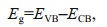
where Eg is the forbidden bandwidth, EVB and ECB are the potentials of the VB and the conduction band (CB) relative to the standard hydrogen electrode (SHE), respectively. Based on the results shown in Fig. 5, the ECB of TiO2 and Cu2O was calculated as -0.55 and -0.64 eV (vs. SHE), respectively.
3.3 PEC and PECCP performances of the prepared photoeletrodesThe PEC performance of the prepared photoelectrodes was studied using a photoinduced volt–ampere characteristic curve (i–V curve) and a photoinduced current density curve (i–t curve), which were tested in 0.1 mol/L Na2SO4 solution under visible light illumination (Fig. 6). Figure 6a depicts the i-t curves of the prepared photoelectrodes, which were obtained at an applied bias potential of 0 V. The currents of TiO2, Cu2O/TiO2-5, Cu2O/TiO2-10, Cu2O/ TiO2-20, and Cu2O/TiO2-30 showed positive shifts when visible light was switched on, indicating that they all exhibit the characteristics of n-type semiconductors (Jing et al., 2019b). However, Cu2O exhibited a negative photocurrent under visible light illumination, indicating that Cu2O prepared at this condition was a p-type semiconductor (Jing et al., 2019b). The pure TiO2 photoelectrode exhibited a small photocurrent density due to its narrower light absorption range. After Cu2O deposition, the photoinduced current densities of the Cu2O/TiO2-X photoelectrodes significantly increased. This could be due to the formation of Cu2O/TiO2 heterojunctions, which accelerated the separation of the photoinduced electron-hole pairs. Thus, the Cu2O/TiO2-X photoelectrodes had higher photochemical conversion performance. The photoinduced current densities increased with the prolongation of the Cu2O deposition time. When the Cu2O deposition time was 20 min, the Cu2O/TiO2-20 had the largest photoinduced current density. With the further prolongation of the Cu2O deposition time to 30 min, the photoinduced current densities of Cu2O/TiO2-30 decreased again. When less electrodeposition time was used, only a small amount of Cu2O deposited and it could not provide sufficient photogenerated electron-hole pairs under visible light. When the Cu2O deposition time was long, a thicker layer of Cu2O was deposited on the surface of TiO2. The over-thick Cu2O coating could remarkably reduce the specific surface area of the photosensitive surface, and the excessive Cu2O could inhibit the effective combination of Cu2O and TiO2; thus the photogenerated electron-hole pairs could not be effectively separated, resulting in a worse photoelectric conversion performance.

|
| Fig.6 The i-t curves (a) and the i-V curves (b) of all the photoeletrodes All these were measured in 0.1 mol/L NaSO4 under visible light in power energy density of 100 mW/cm2. |
Figure 6b shows the i-V curves of the prepared photoelectrodes under intermittent visible light. Pure TiO2 had a small photocurrent density under visible light illumination, while the photocurrent density of Cu2O/TiO2-X increased first and then decreased with the increase of Cu2O deposition time. Cu2O/TiO2-20 had the highest photoinduced current density, which is similar to the change rules of i-t curves shown in Fig. 6a. Cu2O would be oxidized to CuO under more positive voltage, therefore, the i-V curve of Cu2O was scanned to 0 V only. In the whole scanning voltage range, the current density of Cu2O was negative (Fig. 6b).
The PECCP properties of the prepared photoelectrodes were characterized by the photoinduced OCP variations after coupling with 316L SS. Figure 7a & b are the results of the photoinduced OCP variations of the TiO2, Cu2O/TiO2- 5, Cu2O/TiO2-10, Cu2O/TiO2-20, Cu2O/TiO2-30, and Cu2O photoelectrodes coupled with 316L SS, which were measured in 3.5 wt% NaCl solution under intermittent visible light. As shown in Fig. 7a, the photoinduced OCP of the TiO2 nanotubes showed only a small negative shift under visible light because of the narrow light absorption range of TiO2. However, as shown in Fig. 7b, Cu2O exhibited a positive shift of the OCP under visible light illumination, indicating that the electrons transfer from 316L SS to Cu2O and Cu2O alone could not provide PECCP for the coupled 316L SS. However, for Cu2O/TiO2-X, the OCP rapidly shifted to negative direction when the visible light was on, indicating that the photoinduced electrons generated on the CB of Cu2O could be rapidly transferred to the CB of TiO2 under visible light and be further to the coupled 316L SS to provide PECCP. The magnitude of the negative shift of the potential can be used to characterize the PECCP performance of the photoelectrode (Jing et al., 2017). The larger the magnitude of the negative shift of the potential is, the better the PECCP performance is. The photoinduced OCP variation of Cu2O/TiO2-5, Cu2O/ TiO2-10, Cu2O/TiO2-20, and Cu2O/TiO2-30 were 40, 48, 60, and 50 mV, respectively. The Cu2O/TiO2-20 photoelectrode has the largest photoinduced OCP variation under visible light, indicating that 20 min was the optimal Cu2O deposition time and the Cu2O/ TiO2-20 photoelectrode had the best PECCP performance for 316L SS.

|
| Fig.7 Photoinduced OCP variations of the photoelectrodes coupled with 316L SS electrode a. TiO2, Cu2O/TiO2-5, Cu2O/TiO2-10, Cu2O/TiO2-20, and Cu2O/TiO2-30; b. Cu2O. All these were measured in 3.5 wt% NaCl solution under intermittent visible light in power energy density of 100 mW/cm2. |
In addition to the photoinduced potential drop, the PECCP performance of the prepared photoelectrodes could also be characterized by the photoinduced current densities. Figure 8a & b show the variations of the galvanic current densities of the prepared TiO2, Cu2O/TiO2-5, Cu2O/TiO2-10, Cu2O/TiO2-20, Cu2O/ TiO2-30, and Cu2O photoelectrodes coupled with 316L SS in 3.5 wt% NaCl solution under intermittent visible light. A positive photoinduced current density indicates that the photogenerated electrons could be transferred to the coupled 316L SS (Jing et al., 2019b), resulting in the PECCP of the coupled 316L SS. The photoinduced current densities of the TiO2 and Cu2O photoelectrodes were positive and negative, respectively, indicating that TiO2 can provide PECCP while Cu2O cannot provide PECCP for 316L SS, which is consistent with the results of the photoinduced OCP variations shown in Fig. 7. Meanwhile, comparing the photoinduced current densities of Cu2O/TiO2-X composites with different Cu2O deposition times, Cu2O/TiO2-20 had the highest photoinduced current density, indicating that it had the best PECCP performance. These results are also consistent with those of photoinduced OCP variations shown in Fig. 7.

|
| Fig.8 The current densities of the 316L SS electrode coupled with different photoelectrodes a. TiO2, Cu2O/TiO2-5, Cu2O/TiO2-10, Cu2O/TiO2-20, Cu2O/TiO2-30; b. Cu2O under intermittent visible light in power energy density of 100 mW/cm2. |
The ideal PECCP material needs not only good PECCP performance, but also good stability. Figure 9 shows that the photoinduced potential drop of the Cu2O/TiO2-20 photoelectrode coupled with 316L SS in 3.5 wt% NaCl solution under long-term visible light. As shown in Fig. 9, after several cycles of intermittent visible light illumination, the Cu2O/TiO2- 20 photoelectrode coupled with 316L SS electrode was illuminated by visible light for 3.5 h. The potential slowly shifted to positive direction under the visible light. After 3.5 hours of visible light illumination, the positive displacement of the potential was lowered below 20 mV, and the Cu2O/TiO2-20 photoelectrode remained very good PECCP performance. When the light was switched off after a long-term light illumination, the potential rose immediately. When the light was switched on again, the potential decreased immediately, showing good PECCP stability.

|
| Fig.9 Photoinduced OCP of Cu2O/TiO2-20 photoelectrode coupled with 316L SS electrode measured in 3.5 wt% NaCl solution under long-time visible light illumination with the power energy density of 100 mW/cm2 |
To understand the role of deposited Cu2O on improving the PECCP performance of TiO2, the photoluminescence spectroscopy of TiO2 and Cu2O/ TiO2-20 was used to analyze the separation efficiency of the photogenerated electron-hole pairs. The electrons on the VB of the semiconductor material were excited to the CB under light illumination, while leaving the photogenerated holes on the VB. Some of the photogenerated electrons and holes would participate in the PEC reactions; however, most of them would recombine and release energy, which could be detected in photoluminescence spectroscopy. The stronger the peak intensity of the photoluminescence spectrum was, the easier the photogenerated electrons and holes recombine could be. Figure 10a shows the photoluminescence spectra of TiO2 and Cu2O/TiO2-20. The peak intensity of photoluminescence of Cu2O/TiO2-20 was much lower than that of pure TiO2, indicating that Cu2O/TiO2-20 had a much higher separation efficiency of the photogenerated electrons and holes than pure TiO2, which confirms that the Cu2O/TiO2 p-n heterojunctions can effectively separate the photogenerated electronhole pairs.

|
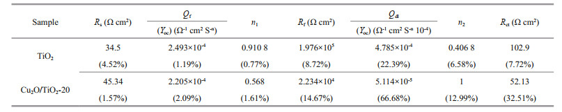
| Fig.10 Photoluminescence spectra of TiO2 and Cu2O/TiO2-20 (a); EIS of TiO2 and Cu2O/TiO2-20 tested in 0.1 mol/L NaSO4 (b) The inset in Fig. 10b is the equivalent electrical circuit used for fitting the EIS data. Rs, Rf, and Rct represent solution resistance, film resistance, and electron transfer resistance, respectively. Q represents a constant phase angle element, and its impedance value was (Y0(jω)n)-1, where ω is the AC voltage angular frequency, Y0 and n are frequency independent parameters. Qf and Qdl represent film capacitor and electric double layer capacitor, respectively. As shown in Fig. 10b, the measured data are the dots with different symbols, while the solid lines are the fitted results using the provided equivalent circuit in the inset. |
The migration ability of the photogenerated carriers of the photoelectrodes could be characterized by EIS. Figure 10b shows the EIS results of TiO2 and Cu2O/TiO2-20 measured in the dark at the OCP. The smaller the radius of the EIS impedance arc is, the larger the migration rates of the photogenerated carriers are. As shown in Fig. 10b, the radius of the impedance arc of Cu2O/TiO2-20 was much smaller than that of pure TiO2, indicating that Cu2O/TiO2-20 had a larger carrier mobility than pure TiO2. To understand why Cu2O/TiO2-20 had higher carrier mobility in detail, the EIS data of TiO2 and Cu2O/TiO2-20 were further fitted by Zismwin software. The insert in Fig. 10b was the corresponding equivalent circuit used for fitting the EIS data. The measured data were fitted very well. Table 1 shows the fitted parameters and the errors of the fitting results of the EIS data. The film resistance and electron transfer resistance of Cu2O/TiO2-20 were greatly reduced compared with those of pure TiO2, indicating that the deposited Cu2O reduced the film resistance of TiO2 and the transfer barrier of interface charge, thus accelerated the electron transfer process and led to a better PEC and PECCP performance.
|
Figure 11 is the proposed mechanism for improving the PEC and PECCP performance by depositing Cu2O on the surface of TiO2. TiO2 is an n-type semiconductor and Cu2O is a p-type semiconductor. The forbidden bandwidth, CB and VB positions of TiO2 are 3.2 eV, -0.55 eV and 2.65 eV, respectively, and those of Cu2O are 2.2 eV, -0.64 eV and 1.56 eV, respectively, which were verified by the results of UV-vis and XPS VB. Under visible light, the electrons on the VB of Cu2O would be excited to the CB of Cu2O, leaving the photogenerated hole on its VB. Since the CB potential of Cu2O is more negative than that of TiO2, the photogenerated electrons on the CB of Cu2O would be transferred to that of TiO2 under visible light, and be further transferred to 316L SS. Therefore, 316L SS was in an electron-rich state, and it was cathodically polarized and the cathodic protection of 316L SS was obtained. Meanwhile, the built-in electric field pointed from TiO2 to Cu2O at the interface of Cu2O/ TiO2 was formed by n-type TiO2 and p-type Cu2O, and this electric field could accelerate the transfer of the photogenerated electrons from the CB of Cu2O to TiO2, which was more favorable to the transfer of the photogenerated electrons to 316L SS. Thus, Cu2O/ TiO2-20 retained much better PEC and PECCP performance.

|
| Fig.11 The proposed mechanism for improving PEC and PECCP of Cu2O/TiO2-20 |
In this paper, TiO2 nanotubes were prepared by anodic oxidation method. Cu2O/TiO2-X composites were prepared by galvanostatic deposition method, and the deposition amount of Cu2O nanoparticles on the surface of TiO2 nanotubes was controlled by the deposition time. The deposition of Cu2O nanoparticles could not only increase the absorption capability of visible light, but also form heterojunctions with TiO2 to improve the separation efficiency of the photogenerated charge carriers. The Cu2O/TiO2-20 photoelectrode had the best PEC and PECCP performance, which should be attributed to the establishment of the built-in electric field at the interface between the p-type Cu2O and n-type TiO2. The built-in electric field accelerated the separation of the photogenerated carriers and pushed more photogenerated electrons to be transferred to 316L SS for PECCP. In addition, the deposition of Cu2O reduced the film resistance of TiO2 and the transfer barrier of interface charge, thus accelerated the electron transfer process and led to a better PEC and PECCP performance. In summary, Cu2O/TiO2 is a feasible visible light-driven PECCP composite material, which provides a new idea for the deposition of Cu2O nanoparticles onto nanotubes or other highly oriented n-type semiconductors to increase the number of photoactive sites, and to further enhance the PEC or PECCP performance under visible light.
5 DATA AVAILABILITY STATEMENTThe experimental and numerical data that support the findings of this study are available from the corresponding author on request.
Aguirre M E, Zhou R X, Eugene A J, Guzman M I, Grela M A. 2017. Cu2O/TiO2 heterostructures for CO2 reduction through a direct Z-scheme:Protecting Cu2O from photocorrosion. Applied Catalysis B:Environmental, 217: 485-493.
DOI:10.1016/j.apcatb.2017.05.058 |
Bu Y Y, Chen Z Y, Ao J P, Hou J, Sun M X. 2018. Study of the photoelectrochemical cathodic protection mechanism for steel based on the SrTiO3-TiO2 composite. Journal of Alloys and Compounds, 731: 1 214-1 224.
DOI:10.1016/j.jallcom.2017.10.165 |
Bu Y Y, Chen Z Y, Yu J Q, Li W B. 2013. A novel application of g-C3N4 thin film in photoelectrochemical anticorrosion. Electrochimica Acta, 88: 294-300.
DOI:10.1016/j.electacta.2012.10.049 |
Chen J, Shen S H, Guo P H, Wang M, Wu P, Wang X X, Guo L J. 2014a. In-situ reduction synthesis of nano-sized Cu2O particles modifying g-C3N4 for enhanced photocatalytic hydrogen production. Applied Catalysis B:Environmental, 52-153: 335-341.
DOI:10.1016/j.apcatb.2014.01.047 |
Chen Y F, Huang W X, He D L, Situ Y, Huang H. 2014b. Construction of heterostructured g-C3N4/Ag/TiO2 microspheres with enhanced photocatalysis performance under visible-light irradiation. ACS Applied Materials & Interfaces, 6(16): 14 405-14 414.
DOI:10.1021/am503674e |
De Jongh P E, Vanmaekelbergh D, Kelly J J. 1999. Cu2O:electrodeposition and characterization. Chemistry of Materials, 11(12): 3 512-3 517.
DOI:10.1021/cm991054e |
Dong J Y, Han J, Liu Y S, Nakajima A, Matsushita S, Wei S H, Gao W. 2014. Defective black TiO2 synthesized via anodization for visible-light photocatalysis. ACS Applied Materials & Interfaces, 6(3): 1 385-1 388.
DOI:10.1021/am405549p |
Foster H A, Ditta I B, Varghese S, Steele A. 2011. Photocatalytic disinfection using titanium dioxide:spectrum and mechanism of antimicrobial activity. Applied Microbiology and Biotechnology, 90(6): 1 847-1 868.
DOI:10.1007/s00253-011-3213-7 |
Fujishima A, Honda K. 1972. Electrochemical photolysis of water at a semiconductor electrode. Nature, 238(5358): 37-38.
DOI:10.1038/238037a0 |
Gou J F, Ma Q L, Deng X Y, Cui Y Q, Zhang H X, Cheng X W, Li X L, Xie M Z, Cheng Q F. 2017. Fabrication of Ag2O/TiO2-Zeolite composite and its enhanced solar light photocatalytic performance and mechanism for degradation of norfloxacin. Chemical Engineering Journal, 308: 818-826.
DOI:10.1016/j.cej.2016.09.089 |
Inguanta R, Piazza S, Sunseri C. 2008. Template electrosynthesis of aligned Cu2O nanowires:Part I. Fabrication and characterization. Electrochimica Acta, 53(22): 6 504-6 512.
DOI:10.1016/j.electacta.2008.04.075 |
Jing J P, Chen Z Y, Bu Y Y, Sun M M, Zheng W Q, Li W B. 2019a. Significantly enhanced photoelectrochemical cathodic protection performance of hydrogen treated Crdoped SrTiO3 by Cr6+ reduction and oxygen vacancy modification. Electrochimica Acta, 304: 386-395.
DOI:10.1016/j.electacta.2019.03.020 |
Jing J P, Chen Z Y, Feng C. 2019b. Dramatically enhanced photoelectrochemical properties and transformed p/n type of g-C3N4 caused by K and I co-doping. Electrochimica Acta, 297: 488-496.
DOI:10.1016/j.electacta.2018.12.015 |
Jing J P, Sun M M, Chen Z Y, Li J R, Xu F L, Xu L K. 2017.Enhanced photoelectrochemical cathodic protection performance of the secondary reduced graphene oxide modified graphitic carbon nitride. Journal of the Electrochemical Society, 164(13): C 822-C 830, DOI: 10.1149/2.1481713jes.
|
Kho Y K, Iwase A, Teoh W Y, Mädler L, Kudo A, Amal R. 2010. Photocatalytic H2 evolution over TiO2 nanoparticles.The synergistic effect of anatase and rutile. The Journal of Physical Chemistry C, 114(6): 2 821-2 829, DOI: 10.1021/jp910810r.
|
Kočí K, Matějů K, Obalová L, Krejčíková S, Lacný Z, Plachá D, Čapek L, Hospodková A, Šolcová O. 2010. Effect of silver doping on the TiO2 for photocatalytic reduction of CO2. Applied Catalysis B: Environmental, 96(3-4): 239-244, DOI: 10.1016/j.apcatb.2010.02.030.
|
Li H, Xia Z B, Chen J Q, Lei L, Xing J H. 2015a. Constructing ternary CdS/reduced graphene oxide/TiO2 nanotube arrays hybrids for enhanced visible-light-driven photoelectrochemical and photocatalytic activity. Applied Catalysis B:Environmental, 168-169: 105-113.
DOI:10.1016/j.apcatb.2014.12.029 |
Li J, Ni Z B, Ji Y J, Zhu Y X, Liu H Z, Zhang Y, Gong X Q, Zhong Z Y, Su F B. 2019. ZnO supported on Cu2O{1 0 0} enhances charge transfer in dimethyldichlorosilane synthesis. Journal of Catalysis, 374: 284-296.
DOI:10.1016/j.jcat.2019.02.029 |
Li Y F, Zhang W P, Shen X, Peng P F, Xiong L B, Yu Y. 2015c. Octahedral Cu2O-modified TiO2 nanotube arrays for efficient photocatalytic reduction of CO2. Chinese Journal of Catalysis, 36(12): 2 229-2 236.
DOI:10.1016/S1872-2067(15)60991-3 |
Li Y P, Wang B W, Liu S H, Duan X F, Hu Z Y. 2015b. Synthesis and characterization of Cu2O/TiO2 photocatalysts for H2 evolution from aqueous solution with different scavengers. Applied Surface Science, 324: 736-744.
DOI:10.1016/j.apsusc.2014.11.027 |
Lu X H, Wang G M, Zhai T, Yu M H, Gan J Y, Tong Y X, Li Y. 2012. Hydrogenated TiO2 nanotube arrays for supercapacitors. Nano Letters, 12(3): 1 690-1 696.
DOI:10.1021/nl300173j |
Lu X H, Yu M H, Wang G M, Zhai T, Xie S L, Ling Y C, Tong Y X, Li Y. 2013. H-TiO2@MnO2//H-TiO2@C core-shell nanowires for high performance and flexible asymmetric supercapacitors. Advanced Materials, 25(2): 267-272.
DOI:10.1002/adma.201203410 |
Momeni M M, Ghayeb Y, Ghonchegi Z. 2015. Fabrication and characterization of copper doped TiO2 nanotube arrays by in situ electrochemical method as efficient visible-light photocatalyst. Ceramics International, 41(7): 8 735-8 741.
DOI:10.1016/j.ceramint.2015.03.094 |
Momeni M M, Ghayeb Y, Moosavi N. 2018. Preparation of Ni-Pt/Fe-TiO2 nanotube films for photoelectrochemical cathodic protection of 403 stainless steel. Nanotechnology, 29(42): 425701.
DOI:10.1088/1361-6528/aad5f5 |
Momeni M M, Khansari-Zadeh S H, Farrokhpour H. 2019a. Fabrication of tungsten-iron-doped TiO2 nanotubes via anodization:new photoelectrodes for photoelectrochemical cathodic protection under visible light. SN Applied Sciences, 1(10): 1 160.
DOI:10.1007/s42452-019-1157-1 |
Momeni M M, Mahvari M, Ghayeb Y. 2019b. Photoelectrochemical properties of iron-cobalt WTiO2 nanotube photoanodes for water splitting and photocathodic protection of stainless steel. Journal of Electroanalytical Chemistry, 832: 7-23.
DOI:10.1016/j.jelechem.2018.10.035 |
Momeni M M, Taghinejad M, Ghayeb Y, Bagheri R, Song Z L. 2019c. Preparation of various boron-doped TiO2 nanostructures by in situ anodizing method and investigation of their photoelectrochemical and photocathodic protection properties. Journal of the Iranian Chemical Society, 16(9): 1 839-1 851.
DOI:10.1007/s13738-019-01658-7 |
Momeni M M. 2015. Fabrication of copper decorated tungsten oxide-titanium oxide nanotubes by photochemical deposition technique and their photocatalytic application under visible light. Applied Surface Science, 357: 160-166.
DOI:10.1016/j.apsusc.2015.09.015 |
Ohko Y, Saitoh S, Tatsuma T, Fujishima A. 2001. Photoelectrochemical anticorrosion and self-cleaning effects of a TiO2 coating for type 304 stainless steel. Journal of the Electrochemical Society, 148(1): B24-B28.
DOI:10.1149/1.1339030 |
Peng B Y, Zhang S S, Yang S Y, Wang H J, Yu H, Zhang S Q, Peng F. 2014. Synthesis and characterization of g-C3N4/Cu2O composite catalyst with enhanced photocatalytic activity under visible light irradiation. Materials Research Bulletin, 56: 19-24.
DOI:10.1016/j.materresbull.2014.04.042 |
Roy P, Kim D, Lee K, Spiecker E, Schmuki P. 2010. TiO2 nanotubes and their application in dye-sensitized solar cells. Nanoscale, 2(1): 45-59.
DOI:10.1039/B9NR00131J |
Sauvage F, Di Fonzo F, Li Bassi A, Casari C S, Russo V, Divitini G, Ducati C, Bottani C E, P. Comte P, Graetzel M. 2010. Hierarchical TiO2 photoanode for dye-sensitized solar cells. Nano Letters, 10(7): 2 562-2 567.
DOI:10.1021/nl101198b |
Sui Y M, Fu W Y, Zeng Y, Yang H B, Zhang Y Y, Chen H, Li Y X, Li M H, Zou G T. 2010. Synthesis of Cu2O nanoframes and nanocages by selective oxidative etching at room temperature. Angewandte Chemie International Edition, 49(25): 4 282-4 285.
DOI:10.1002/anie.200907117 |
Sun M M, Chen Z Y, Bu Y Y, Yu J Q, Hou B R. 2014. Effect of ZnO on the corrosion of zinc, Q235 carbon steel and 304 stainless steel under white light illumination. Corrosion Science, 82: 77-84.
DOI:10.1016/j.corsci.2013.12.022 |
Sun M M, Chen Z Y, Li J R, Hou J, Xu F L, Xu L K, Zeng R C. 2018. Enhanced visible light-driven activity of TiO2 nanotube array photoanode co-sensitized by "green" AgInS2 photosensitizer and In2S3 buffer layer. Electrochimica Acta, 269: 429-440.
DOI:10.1016/j.electacta.2018.03.035 |
Sun M M, Chen Z Y, Yu J Q. 2013. Highly efficient visible light induced photoelectrochemical anticorrosion for 304 SS by Ni-doped TiO2. Electrochimica Acta, 109: 13-19.
DOI:10.1016/j.electacta.2013.07.121 |
Tian B Z, Li C Z, Zhang J L. 2012. One-step preparation, characterization and visible-light photocatalytic activity of Cr-doped TiO2 with anatase and rutile bicrystalline phases. Chemical Engineering Journal, 191: 402-409.
DOI:10.1016/j.cej.2012.03.038 |
Tian J, Chen Z W, Deng X Y, Sun Q, Sun Z Y, Li W B. 2018. Improving visible light driving degradation of norfloxacin over core-shell hierarchical BiOCl microspherical photocatalyst by synergistic effect of oxygen vacancy and nanostructure. Applied Surface Science, 453: 373-382, DOI: 10.1016/j.apsusc.2018.04.255.
|
Wang F Z, Li W J, Gu S N, Li H D, Wu X, Ren C J, Liu X T. 2017. Facile fabrication of direct Z-scheme MoS2/Bi2WO6 heterojunction photocatalyst with superior photocatalytic performance under visible light irradiation. Journal of Photochemistry and Photobiology A:Chemistry, 335: 140-148.
DOI:10.1016/j.jphotochem.2016.11.026 |
Wang W Z, Huang X W, Wu S, Zhou Y X, Wang L J, Shi H L, Liang Y J, Zou B. 2013. Preparation of p-n junction Cu2O/BiVO4 heterogeneous nanostructures with enhanced visible-light photocatalytic activity. Applied Catalysis B:Environmental, 134-135: 293-301.
DOI:10.1016/j.apcatb.2013.01.013 |
Xi Z H, Li C J, Zhang L, Xing M Y, Zhang J L. 2014. Synergistic effect of Cu2O/TiO2 heterostructure nanoparticle and its high H2 evolution activity. International Journal of Hydrogen Energy, 39(12): 6 345-6 353.
DOI:10.1016/j.ijhydene.2014.01.209 |
Xiang Q J, Yu J G, Jaroniec M. 2012. Synergetic effect of MoS2 and graphene as cocatalysts for enhanced photocatalytic H2 production activity of TiO2 nanoparticles. Journal of the American Chemical Society, 134(15): 6 575-6 578.
DOI:10.1021/ja302846n |
Yadav H M, Otari S V, Koli V B, Mali S S, Hong C K, Pawar S H, Delekar S D. 2014. Preparation and characterization of copper-doped anatase TiO2 nanoparticles with visible light photocatalytic antibacterial activity. Journal of Photochemistry and Photobiology A:Chemistry, 280: 32-38.
DOI:10.1016/j.jphotochem.2014.02.006 |
Yan H J, Yang H X. 2011. TiO2-g-C3N4 composite materials for photocatalytic H2 evolution under visible light irradiation. Journal of Alloys and Compounds, 509(4): L26-L29.
DOI:10.1016/j.jallcom.2010.09.201 |
Yang L X, Luo S L, Li Y, Xiao Y, Kang Q, Cai Q Y. 2010. High efficient photocatalytic degradation of p-nitrophenol on a unique Cu2O/TiO2 p-n heterojunction network catalyst. Environmental Science & Technology, 44(19): 7 641-7 646.
DOI:10.1021/es101711k |
Yang Y, Cheng Y F. 2017. Factors affecting the performance and applicability of SrTiO3 photoelectrodes for photoinduced cathodic protection. Journal of the Electrochemical Society, 164(14): C1 067-C1 075.
DOI:10.1149/2.1451714jes |
Yang Y, Cheng Y F. 2018. One-step facile preparation of ZnO nanorods as high-performance photoanodes for photoelectrochemical cathodic protection. Electrochimica Acta, 276: 311-318.
DOI:10.1016/j.electacta.2018.04.206 |
Yao L Z, Wang W Z, Wang L J, Liang Y J, Fu J L, Shi H L. 2018. Chemical bath deposition synthesis of TiO2/Cu2O core/shell nanowire arrays with enhanced photoelectrochemical water splitting for H2 evolution and photostability. International Journal of Hydrogen Energy, 43(33): 15 907-15 917.
DOI:10.1016/j.ijhydene.2018.06.127 |
Zhang Q, Lima D Q, Lee I, Zaera F, Chi M F, Yin Y D. 2011. A highly active titanium dioxide based visible-light photocatalyst with nonmetal doping and plasmonic metal decoration. Angewandte Chemie International Edition, 50(31): 7 088-7 092.
DOI:10.1002/anie.201101969 |
Zhang Z J, Wang W Z, Wang L, Sun S M. 2012. Enhancement of visible-light photocatalysis by coupling with narrowband-gap semiconductor:a case study on Bi2S3/Bi2WO6. ACS Applied Materials & Interfaces, 4(2): 593-597.
DOI:10.1021/am2017199 |
Zhao W, Liu Y, Wei Z B, Yang S G, He H, Sun C. 2016. Fabrication of a novel p-n heterojunction photocatalyst n-BiVO4@p-MoS2 with core-shell structure and its excellent visible-light photocatalytic reduction and oxidation activities. Applied Catalysis B:Environmental, 185: 242-252.
DOI:10.1016/j.apcatb.2015.12.023 |
Zhu C Q, Osherov A, Panzer M J. 2013. Surface chemistry of electrodeposited Cu2O films studied by XPS. Electrochimica Acta, 111: 771-778.
DOI:10.1016/j.electacta.2013.08.038 |
Zhuang J D, Dai W X, Tian Q F, Li Z H, Xie L Y, Wang J X, Liu P, Shi X C, Wang D H. 2010. Photocatalytic degradation of RhB over TiO2 bilayer films:effect of defects and their location. Langmuir, 26(12): 9 686-9 694.
DOI:10.1021/la100302m |